|
|
|
1. Introduction
The assembly of the printing plate is based on the requirements of the design documents and process specifications, and the electronic components are inserted into the printed circuit board according to a certain regularity, and the assembly process is fixed by fasteners or soldering.
2.Specification
| Type | SMT |
| Base material | Copper |
| Flame retardant properties | VO |
| Item number | PCB Manufacturer |
| Brand | PCBA circuit board electronic component assembly |
| Layer | 2 |
| Customized | Yes |
| Processing technology | Electrolytic foil |
3. Application
PCBs can be single-sided (one copper layer), double-sided (two copper layers on both sides of one substrate layer), or multi-layer (outer and inner layers of copper, alternating with layers of substrate). Multi-layer PCBs allow for much higher component density, because circuit traces on the inner layers would otherwise take up surface space between components. The rise in popularity of multilayer PCBs with more than two, and especially with more than four, copper planes was concurrent with the adoption of surface mount technology. However, multilayer PCBs make repair, analysis, and field modification of circuits much more difficult and usually impractical.
Product Details:
Payment & Shipping Terms:
|
| Layer Count: | 2 ` 30 Layers | Max Board Size: | 600 Mm X 1200 Mm |
|---|---|---|---|
| Base Material For PCB: | FR4, CEM-1, TACONIC, Aluminium, High Tg Material, High Frequence ROGERS ,TEFLON, ARLON, Halogen-free Material | Rang Of Finish Baords Thickness: | 0.21-7.0mm |
| Minimum Line Width: | 3mil (0.075mm) | Minimum Line Space: | 3mil (0.075mm) |
| Minimum Hole Diameter: | 0.10 Mm | Finishing Treatment: | HASL (Tin-Lead Free), ENIG(Immersion Gold), Immersion Silver , Gold Plating (Flash Gold), OSP, Etc. |
| Thickness Of Copper: | 0.5-14oz (18-490um) | E-Testing: | 100% E-Testing (High Voltage Testing); Flying Probe Testing |
| Layers: | 6Layers | Copper: | 2OZ |
| Material: | FR4 | Surface: | ENIG/HASL |
| High Light: | FR4 Electronic Circuit Board Assembly,SMT Electronic Circuit Board Assembly |
||
FR4 Material SMT Prototype PCB Assembly Service ENIG HASL Surface
OEM ODM service offer gsm security PCB design/electronic chart design developing
1. Description Of PCB Assembly Service
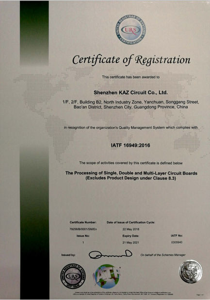
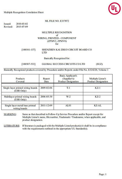
PCB Assembly is 4 layer it is used for security equipment application. we can accept PCB prototype,samll volum, middle and large volume. no MOQ request for new order.all of our PCB are met UL, TS 16949,ROHS, ISO etc. certification.
2. Specification Of PCB Assembly Service
| 1 | Layer | 1-30 layer |
| 2 | Material | FR-4, CEM-1, CEM-3, Hight TG, FR4 Halogen Free, FR-1, FR-2, Aluminum |
| 3 | Board thickness | 0.2mm-7mm |
| 4 | Max.finished board side | 500mm*500mm |
| 5 | Min.drilled hole size | 0.25mm |
| 6 | Min.line width | 0.075mm(3mil) |
| 7 | Min.line spaceing | 0.075mm(3mil) |
| 8 | Surface finish/treatment | HALS/HALS lead free, Chemical tin, Chemical Gold, Immersion gold Inmersion Silver/Gold, Osp, Gold Plating |
| 9 | Copper thickness | 0.5-4.0oz |
| 10 | Solder mask color | green/black/white/red/blue/yellow |
| 11 | Inner packing | Vacuum packing, Plastic bag |
| 12 | Outer packing | Standard carton packing |
| 13 | Hole tolerance | PTH:±0.076, NTPH:±0.05 |
| 14 | Certificate | UL, ISO9001, ISO14001, ROHS, CQC |
| 15 | Profiling Punching | Routing, V-CUT, Beveling |
| 16 | Assembly Service | Providing OEM service to all sorts of printed circuit board assembly |
3. Products Application:
1, Telecom Communication
2, Consumer Electronics
3, Security monitor
4, Vehicle Electronices
5, Smart Home
6, Industrial controls
7, Military & Defense
8, Automotive
9, Smart Home
10, Industrial Automation
11, Medical Devices
12, New Energy
And so on
4. Advantage Of PCB Assembly Service
• Strict product liability, taking IPC-A-160 standard
• Engineering pretreatment before production
• Production process control (5Ms)
• 100% E-test, 100% visual inspection, including IQC, IPQC, FQC, OQC
• 100% AOI inspection, including X-ray, 3D microscope and ICT
• High-voltage test, impedance control test
• Micro section, soldering capacity, thermal stress test, shocking test
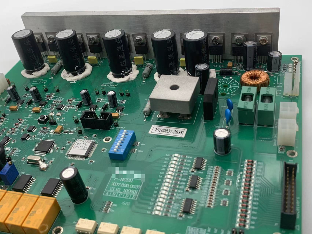
5. Picture
![]()
![]()
![]()
6. OEM/ODM/EMS Services For PCBA:
· PCBA, PCB Board assembly: SMT & PTH & BGA
· PCBA and enclosure design
· Components sourcing and purchasing
· Quick prototyping
· Plastic injection molding
· Metal sheet stamping
· Final assembly
· Test: AOI, In-Circuit Test (ICT), Functional Test (FCT)
· Custom clearance for material importing and product exporting
FAQ
Q1: Are you a factory or trading company?
-----We are a factory,Our company is printed circuit board manufacturers
Q2: Do you accept sample order?
------Yes, we can accept sample order.
Q3: What's your warranty policy?
-----We offer 2 year warranty. For goods defected not by personal seasons, we will replace for it.
Q4: What's your payment terms?
------We accept T/T in advance, paypal, or alipay account.
Q5:What's the lead time for mass order?
------Normally, it takes about 20-35 days, depends on the order quantity.
Contact Person: Mrs. Helen Jiang
Tel: 86-18118756023
Fax: 86-755-85258059